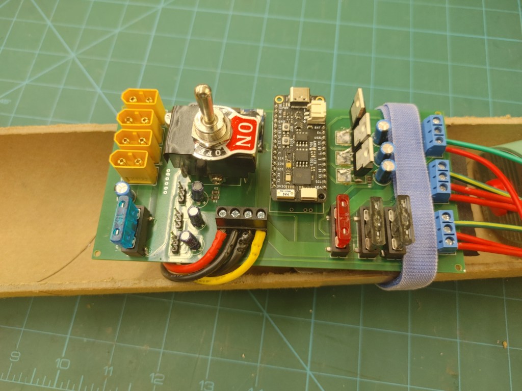
My team is currently designing a bouyancy-driven underwater glider following design specifications laid out in the N231-032 ONR call for proposals. To support that project, I designed a PCB for enabling intermediate testing steps while the final PCB is being designed by a student.
The design is currently in rev 11, less than 8 weeks after starting, an extreme pace for any product development schedule. The final prototyped design was generated by Neera Raychaudhuri, who not only learned MultiSim and UltiBoard in that time, but also kept up with the tight schedule.

The PCB artwork for the submarine control board
Design considerations
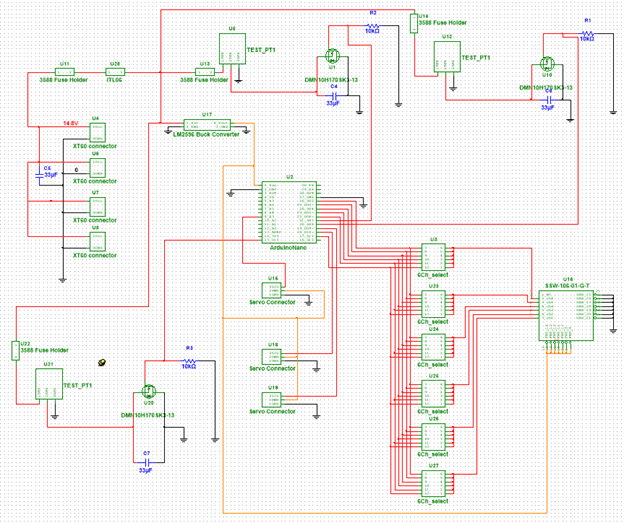
The high-power PCB provides support for two 12V 12W hydraulic solenoid valves, a 12V 120W hydraulic pump, two 12V frequency-controlled servos, a 1.6MPa water pressure sensor, a LoRa radio transceiver built into a RadioFruit microcontroller. The design includes a high current power bus, permitting up to 20A for a temperature rise no higher than 20C, all packaged within a roughly 10cm x 15cm area. This design also features redundant fuse protection and power spike balancing with electrolytic capacitors. The first version used a 2.4GHz receiver instead with jumpers to control which channel went to which microcontroller pin, but this approach was later abandoned in favor of the LoRa platform.
Nearly every schematic symbol and layout footprint is custom designed. While this is not standard practice, in this case it was done to carefully manage the component database for use by the student team. This way, silkscreen identifiers can be used to ease assembly of both the schematic and final, physical board.
As with all student-facing designs, this design uses a mix of mounting technologies, features generic parts, and is configured to aid rapid learning and retention.

First article inspection
First article inspection revealed a single error on the board which was easily resolved by joining two microcontroller pins with a soldered jumper. We also discovered that we had designed the footprint for the fuse holders and MOSFET’s differently than the parts we had specified, but we were able to deadbug the MOSFET’s with through-hole equivalents and reorder the correct fuse holders, allowing us to finish on the accelerated schedule.

The first prototyped board. This board was used for determining fit and function and includes some traces and components that were broken during troubleshooting. The final board is shown at the top of this post.
Leave a comment